|
Shaping Processes In Crystal Growth
Shaping processes in crystal growth are a collection of techniques for growing bulk crystals of a defined shape from a melt, usually by constraining the shape of the liquid meniscus by means of a mechanical shaper. Crystals are commonly grown as fibers, solid cylinders, hollow cylinders (or tubes), and sheets (or plates). More complex shapes such as tubes with a complex cross section, and domes have also been produced.Dobrovinskaya, Elena R., Leonid A. Lytvynov, and Valerian Pishchik. Sapphire: material, manufacturing, applications. Springer Science & Business Media, 2009. Using a shaping process can produce a near net shape crystal and reduce the manufacturing cost for crystals which are composed of very expensive or difficult to machine materials. List of shaping processes * Horizontal Ribbon Growth (HRG, 1959) *Edge-defined Film-fed Growth (EFG, 1960) *Low Angle Silicon Sheet (LASS, 1981) * Micro-pulling-down (µ-PD) * Stepanov technique * String ribbon Edge-defined film-fe ... [...More Info...] [...Related Items...] OR: [Wikipedia] [Google] [Baidu] |
Crystals
A crystal or crystalline solid is a solid material whose constituents (such as atoms, molecules, or ions) are arranged in a highly ordered microscopic structure, forming a crystal lattice that extends in all directions. In addition, macroscopic single crystals are usually identifiable by their geometrical shape, consisting of flat faces with specific, characteristic orientations. The scientific study of crystals and crystal formation is known as crystallography. The process of crystal formation via mechanisms of crystal growth is called crystallization or solidification. The word ''crystal'' derives from the Ancient Greek word (), meaning both "ice" and "rock crystal", from (), "icy cold, frost". Examples of large crystals include snowflakes, diamonds, and table salt. Most inorganic solids are not crystals but polycrystals, i.e. many microscopic crystals fused together into a single solid. Polycrystals include most metals, rocks, ceramics, and ice. A third category of s ... [...More Info...] [...Related Items...] OR: [Wikipedia] [Google] [Baidu] |
Infrared
Infrared (IR), sometimes called infrared light, is electromagnetic radiation (EMR) with wavelengths longer than those of visible light. It is therefore invisible to the human eye. IR is generally understood to encompass wavelengths from around 1 millimeter (300 GHz) to the nominal red edge of the visible spectrum, around 700 nanometers (430 THz). Longer IR wavelengths (30 μm-100 μm) are sometimes included as part of the terahertz radiation range. Almost all black-body radiation from objects near room temperature is at infrared wavelengths. As a form of electromagnetic radiation, IR propagates energy and momentum, exerts radiation pressure, and has properties corresponding to both those of a wave and of a particle, the photon. It was long known that fires emit invisible heat; in 1681 the pioneering experimenter Edme Mariotte showed that glass, though transparent to sunlight, obstructed radiant heat. In 1800 the astronomer Sir William Herschel discovered ... [...More Info...] [...Related Items...] OR: [Wikipedia] [Google] [Baidu] |
Indium Antimonide
Indium antimonide (InSb) is a crystalline compound made from the elements indium (In) and antimony (Sb). It is a narrow- gap semiconductor material from the III- V group used in infrared detectors, including thermal imaging cameras, FLIR systems, infrared homing missile guidance systems, and in infrared astronomy. The indium antimonide detectors are sensitive between 1–5 μm wavelengths. Indium antimonide was a very common detector in the old, single-detector mechanically scanned thermal imaging systems. Another application is as a terahertz radiation source as it is a strong photo-Dember emitter. History The intermetallic compound was first reported by Liu and Peretti in 1951, who gave its homogeneity range, structure type, and lattice constant. Polycrystalline ingots of InSb were prepared by Heinrich Welker in 1952, although they were not very pure by today's semiconductor standards. Welker was interested in systematically studying the semiconducting properties of t ... [...More Info...] [...Related Items...] OR: [Wikipedia] [Google] [Baidu] |
III-V Semiconductors
Semiconductor materials are nominally small band gap insulators. The defining property of a semiconductor material is that it can be compromised by doping it with impurities that alter its electronic properties in a controllable way. Because of their application in the computer and photovoltaic industry—in devices such as transistors, lasers, and solar cells—the search for new semiconductor materials and the improvement of existing materials is an important field of study in materials science. Most commonly used semiconductor materials are crystalline inorganic solids. These materials are classified according to the periodic table groups of their constituent atoms. Different semiconductor materials differ in their properties. Thus, in comparison with silicon, compound semiconductors have both advantages and disadvantages. For example, gallium arsenide (GaAs) has six times higher electron mobility than silicon, which allows faster operation; wider band gap, which allo ... [...More Info...] [...Related Items...] OR: [Wikipedia] [Google] [Baidu] |
William Shockley
William Bradford Shockley Jr. (February 13, 1910 – August 12, 1989) was an American physicist and inventor. He was the manager of a research group at Bell Labs that included John Bardeen and Walter Brattain. The three scientists were jointly awarded the 1956 Nobel Prize in Physics for "their researches on semiconductors and their discovery of the transistor effect". Partly as a result of Shockley's attempts to commercialize a new transistor design in the 1950s and 1960s, California's Silicon Valley became a hotbed of electronics innovation. In his later life, while a professor of electrical engineering at Stanford University and afterward, Shockley became widely known for his racist views and advocacy of eugenics. Early life and education Shockley was born to American parents in London on February 13, 1910, and was raised in his family's hometown of Palo Alto, California, from the age of three. His father, William Hillman Shockley, was a mining engineer who speculated in ... [...More Info...] [...Related Items...] OR: [Wikipedia] [Google] [Baidu] |
Iridium
Iridium is a chemical element with the symbol Ir and atomic number 77. A very hard, brittle, silvery-white transition metal of the platinum group, it is considered the second-densest naturally occurring metal (after osmium) with a density of as defined by experimental X-ray crystallography. It is one of the most corrosion-resistant metals, even at temperatures as high as . However, corrosion-resistance is not quantifiable in absolute terms; although only certain molten salts and halogens are corrosive to solid iridium, finely divided iridium dust is much more reactive and can be flammable, whereas gold dust is not flammable but can be attacked by substances that iridium resists, such as aqua regia. Iridium was discovered in 1803 among insoluble impurities in natural platinum. Smithson Tennant, the primary discoverer, named it after the Greek goddess Iris, personification of the rainbow, because of the striking and diverse colors of its salts. Iridium is one of the rarest ... [...More Info...] [...Related Items...] OR: [Wikipedia] [Google] [Baidu] |
Lithium Niobate
Lithium niobate () is a non-naturally-occurring salt consisting of niobium, lithium, and oxygen. Its single crystals are an important material for optical waveguides, mobile phones, piezoelectric sensors, optical modulators and various other linear and non-linear optical applications. Lithium niobate is sometimes referred to by the brand name linobate. Properties Lithium niobate is a colorless solid, and it is insoluble in water. It has a trigonal crystal system, which lacks inversion symmetry and displays ferroelectricity, the Pockels effect, the piezoelectric effect, photoelasticity and nonlinear optical polarizability. Lithium niobate has negative uniaxial birefringence which depends slightly on the stoichiometry of the crystal and on temperature. It is transparent for wavelengths between 350 and 5200 nanometers. Lithium niobate can be doped by magnesium oxide, which increases its resistance to optical damage (also known as photorefractive damage) when doped above the optica ... [...More Info...] [...Related Items...] OR: [Wikipedia] [Google] [Baidu] |
Gallium(III) Oxide
Gallium(III) oxide is an inorganic compound and ultra-wide bandgap semiconductor with the formula Ga2 O3. It is actively studied for applications in power electronics, phosphors, and gas sensing. The compound has several polymorphs, of which the monoclinic β-phase is the most stable. The β-phase’s bandgap of 4.7–4.9 eV and large-area, native substrates make it a promising competitor to GaN and SiC-based power electronics applications and solar-blind UV photodetectors. Ga2O3 exhibits reduced thermal conductivity and electron mobility by an order of magnitude compared to GaN and SiC, but is predicted to be significantly more cost-effective due to being the only wide-bandgap material capable of being grown from melt. β-Ga2O3 is thought to be radiation hard which makes it promising for military and space applications. Preparation Gallium trioxide is precipitated in hydrated form upon neutralization of acidic or basic solution of gallium salt. Also, it is formed on heat ... [...More Info...] [...Related Items...] OR: [Wikipedia] [Google] [Baidu] |
Graphite
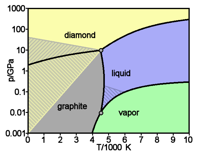
Graphite () is a crystalline form of the element carbon. It consists of stacked layers of graphene. Graphite occurs naturally and is the most stable form of carbon under standard conditions. Synthetic and natural graphite are consumed on large scale (300 kton/year, in 1989) for uses in pencils, lubricants, and electrodes. Under high pressures and temperatures it converts to diamond. It is a weak conductor of heat and electricity. Types and varieties Natural graphite The principal types of natural graphite, each occurring in different types of ore deposits, are * Crystalline small flakes of graphite (or flake graphite) occurs as isolated, flat, plate-like particles with hexagonal edges if unbroken. When broken the edges can be irregular or angular; * Amorphous graphite: very fine flake graphite is sometimes called amorphous; * Lump graphite (or vein graphite) occurs in fissure veins or fractures and appears as massive platy intergrowths of fibrous or acicular crystalline ... [...More Info...] [...Related Items...] OR: [Wikipedia] [Google] [Baidu] |
Solar Photovoltaic
A photovoltaic system, also PV system or solar power system, is an electric power system designed to supply usable solar power by means of photovoltaics. It consists of an arrangement of several components, including solar panels to absorb and convert sunlight into electricity, a solar inverter to convert the output from direct to alternating current, as well as mounting, cabling, and other electrical accessories to set up a working system. It may also use a solar tracking system to improve the system's overall performance and include an integrated battery. PV systems convert light directly into electricity, and are not to be confused with other solar technologies, such as concentrated solar power or solar thermal, used for heating and cooling. A solar array only encompasses the ensemble of solar panels, the visible part of the PV system, and does not include all the other hardware, often summarized as balance of system (BOS). PV systems range from small, rooftop-mounted or ... [...More Info...] [...Related Items...] OR: [Wikipedia] [Google] [Baidu] |
Silicon
Silicon is a chemical element with the symbol Si and atomic number 14. It is a hard, brittle crystalline solid with a blue-grey metallic luster, and is a tetravalent metalloid and semiconductor. It is a member of group 14 in the periodic table: carbon is above it; and germanium, tin, lead, and flerovium are below it. It is relatively unreactive. Because of its high chemical affinity for oxygen, it was not until 1823 that Jöns Jakob Berzelius was first able to prepare it and characterize it in pure form. Its oxides form a family of anions known as silicates. Its melting and boiling points of 1414 °C and 3265 °C, respectively, are the second highest among all the metalloids and nonmetals, being surpassed only by boron. Silicon is the eighth most common element in the universe by mass, but very rarely occurs as the pure element in the Earth's crust. It is widely distributed in space in cosmic dusts, planetoids, and planets as various forms of silicon dioxide ( ... [...More Info...] [...Related Items...] OR: [Wikipedia] [Google] [Baidu] |


