|
JFET
The junction-gate field-effect transistor (JFET) is one of the simplest types of field-effect transistor. JFETs are three-terminal semiconductor devices that can be used as electronically controlled switches or resistors, or to build amplifiers. Unlike bipolar junction transistors, JFETs are exclusively voltage-controlled in that they do not need a biasing current. Electric charge flows through a semiconducting channel between ''source'' and ''drain'' terminals. By applying a reverse bias voltage to a ''gate'' terminal, the channel is ''pinched'', so that the electric current is impeded or switched off completely. A JFET is usually conducting when there is zero voltage between its gate and source terminals. If a potential difference of the proper polarity is applied between its gate and source terminals, the JFET will be more resistive to current flow, which means less current would flow in the channel between the source and drain terminals. JFETs are sometimes referred to as ... [...More Info...] [...Related Items...] OR: [Wikipedia] [Google] [Baidu] |
Voltage-controlled Resistor
A voltage-controlled resistor (VCR) is a three-terminal active device with one input port and two output ports. The input-port voltage controls the value of the resistor between the output ports. VCRs are most often built with field-effect transistors (FETs). Two types of FETs are often used: the JFET and the MOSFET. There are both Floating ground, floating voltage-controlled resistors and grounded voltage-controlled resistors. Floating VCRs can be placed between two passive or active components. Grounded VCRs, the more common and less complicated design, require that one port of the voltage-controlled resistor be grounded. Usages Voltage-controlled resistors are one of the most commonly used analog design blocks: adaptive analog filters, automatic gain-control circuits, clock generators, compressors, electrometers, energy harvesters, expanders, hearing aids, light dimmers, modulators (mixers), artificial neural networks, programmable-gain amplifiers, phased arrays, phase-locked l ... [...More Info...] [...Related Items...] OR: [Wikipedia] [Google] [Baidu] |
Field-effect Transistor
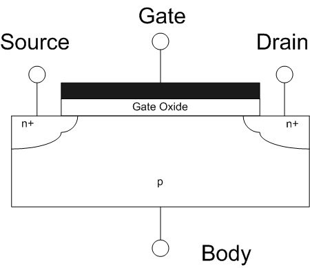
The field-effect transistor (FET) is a type of transistor that uses an electric field to control the flow of current in a semiconductor. FETs (JFETs or MOSFETs) are devices with three terminals: ''source'', ''gate'', and ''drain''. FETs control the flow of current by the application of a voltage to the gate, which in turn alters the conductivity between the drain and source. FETs are also known as unipolar transistors since they involve single-carrier-type operation. That is, FETs use either electrons (n-channel) or holes (p-channel) as charge carriers in their operation, but not both. Many different types of field effect transistors exist. Field effect transistors generally display very high input impedance at low frequencies. The most widely used field-effect transistor is the MOSFET (metal-oxide-semiconductor field-effect transistor). History The concept of a field-effect transistor (FET) was first patented by Austro-Hungarian physicist Julius Edgar Lilienfeld in 192 ... [...More Info...] [...Related Items...] OR: [Wikipedia] [Google] [Baidu] |
IEEE 315-1975 (1993) 8
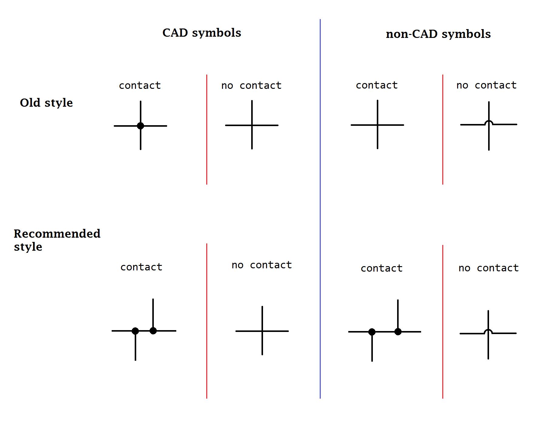
An electronic symbol is a pictogram used to represent various electrical and electronic devices or functions, such as wires, batteries, resistors, and transistors, in a schematic diagram of an electrical or electronic circuit. These symbols are largely standardized internationally today, but may vary from country to country, or engineering discipline, based on traditional conventions. Standards for symbols The graphic symbols used for electrical components in circuit diagram A circuit diagram (wiring diagram, electrical diagram, elementary diagram, electronic schematic) is a graphical representation of an electrical circuit. A pictorial circuit diagram uses simple images of components, while a schematic diagram s ...s are covered by national and international standards, in particular: * International Electrotechnical Commission, IEC 60617 (also known as British Standard, BS 3939). * There is also IEC 61131-3 – for ladder-logic symbols. * Joint industrial council, JIC JIC ... [...More Info...] [...Related Items...] OR: [Wikipedia] [Google] [Baidu] |
Common Source
In electronics, a common-source amplifier is one of three basic single-stage field-effect transistor (FET) amplifier topologies, typically used as a voltage or transconductance amplifier. The easiest way to tell if a FET is common source, common drain, or common gate is to examine where the signal enters and leaves. The remaining terminal is what is known as "common". In this example, the signal enters the gate, and exits the drain. The only terminal remaining is the source. This is a common-source FET circuit. The analogous bipolar junction transistor circuit may be viewed as a transconductance amplifier or as a voltage amplifier. (See classification of amplifiers). As a transconductance amplifier, the input voltage is seen as modulating the current going to the load. As a voltage amplifier, input voltage modulates the current flowing through the FET, changing the voltage across the output resistance according to Ohm's law. However, the FET device's output resistance typicall ... [...More Info...] [...Related Items...] OR: [Wikipedia] [Google] [Baidu] |
Common Drain
In electronics, a common-drain amplifier, also known as a source follower, is one of three basic single-stage field-effect transistor (FET) amplifier topologies, typically used as a voltage buffer. In this circuit (NMOS) the gate terminal of the transistor serves as the signal input, the source is the output, and the drain is ''common'' to both (input and output), hence its name. The analogous bipolar junction transistor circuit is the common-collector amplifier. This circuit is also commonly called a "stabilizer". In addition, this circuit is used to transform impedances. For example, the Thévenin resistance of a combination of a voltage follower driven by a voltage source with high Thévenin resistance is reduced to only the output resistance of the voltage follower (a small resistance). That resistance reduction makes the combination a more ideal voltage source. Conversely, a voltage follower inserted between a driving stage and a high load (i.e. a low resistance) presents a ... [...More Info...] [...Related Items...] OR: [Wikipedia] [Google] [Baidu] |
N-type Semiconductor
An extrinsic semiconductor is one that has been '' doped''; during manufacture of the semiconductor crystal a trace element or chemical called a doping agent has been incorporated chemically into the crystal, for the purpose of giving it different electrical properties than the pure semiconductor crystal, which is called an ''intrinsic semiconductor''. In an extrinsic semiconductor it is these foreign dopant atoms in the crystal lattice that mainly provide the charge carriers which carry electric current through the crystal. The doping agents used are of two types, resulting in two types of extrinsic semiconductor. An ''electron donor'' dopant is an atom which, when incorporated in the crystal, releases a mobile conduction electron into the crystal lattice. An extrinsic semiconductor which has been doped with electron donor atoms is called an n-type semiconductor, because the majority of charge carriers in the crystal are negative electrons. An ''electron acceptor'' dopant is ... [...More Info...] [...Related Items...] OR: [Wikipedia] [Google] [Baidu] |
P-type Semiconductor
An extrinsic semiconductor is one that has been '' doped''; during manufacture of the semiconductor crystal a trace element or chemical called a doping agent has been incorporated chemically into the crystal, for the purpose of giving it different electrical properties than the pure semiconductor crystal, which is called an ''intrinsic semiconductor''. In an extrinsic semiconductor it is these foreign dopant atoms in the crystal lattice that mainly provide the charge carriers which carry electric current through the crystal. The doping agents used are of two types, resulting in two types of extrinsic semiconductor. An ''electron donor'' dopant is an atom which, when incorporated in the crystal, releases a mobile conduction electron into the crystal lattice. An extrinsic semiconductor which has been doped with electron donor atoms is called an n-type semiconductor, because the majority of charge carriers in the crystal are negative electrons. An ''electron acceptor'' dopant is ... [...More Info...] [...Related Items...] OR: [Wikipedia] [Google] [Baidu] |
Channel Length Modulation
Channel length modulation (CLM) is an effect in field effect transistors, a shortening of the length of the inverted channel region with increase in drain bias for large drain biases. The result of CLM is an increase in current with drain bias and a reduction of output resistance. It is one of several short-channel effects in MOSFET scaling. It also causes distortion in JFET amplifiers. To understand the effect, first the notion of pinch-off of the channel is introduced. The channel is formed by attraction of carriers to the gate, and the current drawn through the channel is nearly a constant independent of drain voltage in saturation mode. However, near the drain, the gate ''and drain'' jointly determine the electric field pattern. Instead of flowing in a channel, beyond the pinch-off point the carriers flow in a subsurface pattern made possible because the drain and the gate both control the current. In the figure at the right, the channel is indicated by a dashed line and beco ... [...More Info...] [...Related Items...] OR: [Wikipedia] [Google] [Baidu] |
Depletion-mode
In field-effect transistors (FETs), depletion mode and enhancement mode are two major transistor types, corresponding to whether the transistor is in an on state or an off state at zero gate–source voltage. Enhancement-mode MOSFETs (metal–oxide–semiconductor FETs) are the common switching elements in most integrated circuits. These devices are off at zero gate–source voltage. NMOS can be turned on by pulling the gate voltage higher than the source voltage, PMOS can be turned on by pulling the gate voltage lower than the source voltage. In most circuits, this means pulling an enhancement-mode MOSFET's gate voltage towards its drain voltage turns it on. In a depletion-mode MOSFET, the device is normally on at zero gate–source voltage. Such devices are used as load "resistors" in logic circuits (in depletion-load NMOS logic, for example). For N-type depletion-load devices, the threshold voltage might be about −3 V, so it could be turned off by pulling the gate 3&nb ... [...More Info...] [...Related Items...] OR: [Wikipedia] [Google] [Baidu] |
Biasing
In electronics, biasing is the setting of DC (direct current) operating conditions (current and voltage) of an active device in an amplifier. Many electronic devices, such as diodes, transistors and vacuum tubes, whose function is processing time-varying ( AC) signals, also require a steady (DC) current or voltage at their terminals to operate correctly. This current or voltage is called ''bias''. The AC signal applied to them is superposed on this DC bias current or voltage. The operating point of a device, also known as bias point, quiescent point, or Q-point, is the DC voltage or current at a specified terminal of an active device (a transistor or vacuum tube) with no input signal applied. A bias circuit is a portion of the device's circuit which supplies this steady current or voltage. Overview In electronics, 'biasing' usually refers to a fixed DC voltage or current applied to a terminal of an electronic component such as a diode, transistor or vacuum tube in a circuit ... [...More Info...] [...Related Items...] OR: [Wikipedia] [Google] [Baidu] |
Electric Current
An electric current is a stream of charged particles, such as electrons or ions, moving through an electrical conductor or space. It is measured as the net rate of flow of electric charge through a surface or into a control volume. The moving particles are called charge carriers, which may be one of several types of particles, depending on the conductor. In electric circuits the charge carriers are often electrons moving through a wire. In semiconductors they can be electrons or holes. In an electrolyte the charge carriers are ions, while in plasma, an ionized gas, they are ions and electrons. The SI unit of electric current is the ampere, or ''amp'', which is the flow of electric charge across a surface at the rate of one coulomb per second. The ampere (symbol: A) is an SI base unit. Electric current is measured using a device called an ammeter. Electric currents create magnetic fields, which are used in motors, generators, inductors, and transformers. In ordinary con ... [...More Info...] [...Related Items...] OR: [Wikipedia] [Google] [Baidu] |
Julius Edgar Lilienfeld
Julius Edgar Lilienfeld (April 18, 1882 – August 28, 1963) was an Austro-Hungarian, and later American (where he moved in 1921) physicist and electrical engineer, who was credited with the first patent on the field-effect (FET) (1925). Because of his failure to publish articles in learned journals and because high-purity semiconductor materials were not available yet, his FET patent never achieved fame, causing confusion for later inventors. Early life Lilienfeld was born into a German-speaking Ashkenazi Jewish family in Lemberg (present-day Lviv) in the Austrian part of the Austro-Hungarian Empire. Education Between 1900 and 1904, Lilienfeld studied at the Friedrich-Wilhelms-Universität (renamed Humboldt University in 1949), in Berlin, where he received his Ph.D. on February 18, 1905. In 1905, he started work at the physics institute at Leipzig University as an untenured professor. Career Lilienfeld's early career, at the University of Leipzig, saw him conduct impor ... [...More Info...] [...Related Items...] OR: [Wikipedia] [Google] [Baidu] |


