|
Embedded Wafer Level Ball Grid Array
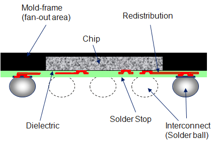
Embedded wafer level ball grid array (eWLB) is a packaging technology for integrated circuits. The package interconnects are applied on an artificial wafer made of silicon chips and a casting compound. eWLB is a further development of the classical wafer level ball grid array technology (WLB or WLP: wafer level package). The main driving force behind the eWLB technology was to allow fanout and more space for interconnect routing. All process steps for the generation of the package are performed on the wafer. This allows, in comparison to classical packaging technologies (e. g. ball grid array), the generation of very small and flat packages with excellent electrical and thermal performance at lowest cost. It is common for all WLB technologies, which are built on a silicon wafer, that the interconnects (typically solder balls) fit on the chip (so called fan-in design). Therefore only chips with a restricted number of interconnects can be packaged. The eWLB technology allows the ... [...More Info...] [...Related Items...] OR: [Wikipedia] [Google] [Baidu] |
EWLB Sketch E
Embedded wafer level ball grid array (eWLB) is a packaging technology for integrated circuits. The package interconnects are applied on an artificial wafer made of silicon chips and a casting compound. eWLB is a further development of the classical wafer level ball grid array technology (WLB or WLP: wafer level package). The main driving force behind the eWLB technology was to allow fanout and more space for interconnect routing. All process steps for the generation of the package are performed on the wafer. This allows, in comparison to classical packaging technologies (e. g. ball grid array), the generation of very small and flat packages with excellent electrical and thermal performance at lowest cost. It is common for all WLB technologies, which are built on a silicon wafer, that the interconnects (typically solder balls) fit on the chip (so called fan-in design). Therefore only chips with a restricted number of interconnects can be packaged. The eWLB technology allows the ... [...More Info...] [...Related Items...] OR: [Wikipedia] [Google] [Baidu] |
Wafer Level Package
Wafer-level packaging (WLP) is a process where packaging components are attached to an integrated circuit (IC) ''before'' the wafer – on which the IC is fabricated – is diced. In WSP, the top and bottom layers of the packaging and the solder bumps are attached to the integrated circuits while they are still in the wafer. This process differs from a conventional process, in which the wafer is sliced into individual circuits (dice) before the packaging components are attached. WLP is essentially a true chip-scale package (CSP) technology, since the resulting package is practically of the same size as the die. Wafer-level packaging allows integration of wafer fab, packaging, test, and burn-in at wafer level in order to streamline the manufacturing process undergone by a device from silicon start to customer shipment. There is no single industry-standard method of wafer-level packaging at present. A major application area of WLPs are smartphones due to the size constraints. For e ... [...More Info...] [...Related Items...] OR: [Wikipedia] [Google] [Baidu] |
Ball Grid Array
A ball grid array (BGA) is a type of surface-mount packaging (a chip carrier) used for integrated circuits. BGA packages are used to permanently mount devices such as microprocessors. A BGA can provide more interconnection pins than can be put on a dual in-line or flat package. The whole bottom surface of the device can be used, instead of just the perimeter. The traces connecting the package's leads to the wires or balls which connect the die to package are also on average shorter than with a perimeter-only type, leading to better performance at high speeds. BGAs were introduced in the 1990s and became popular by 2001. Soldering of BGA devices requires precise control and is usually done by automated processes such as in computer-controlled automatic reflow ovens. Description The BGA is descended from the pin grid array (PGA), which is a package with one face covered (or partly covered) with pins in a grid pattern which, in operation, conduct electrical signals betwe ... [...More Info...] [...Related Items...] OR: [Wikipedia] [Google] [Baidu] |
Solder Ball
In integrated circuit packaging, a solder ball, also a solder bump (ofter referred to simply as "ball" or "bumps") is a ball of solder that provides the contact between the chip package and the printed circuit board, as well as between stacked packages in multichip modules; in the latter case, they may be referred to as microbumps (μbumps, ubumps), since they are usually significantly smaller than the former. The solder balls can be placed manually or by automated equipment, and are held in place with a tacky flux. A coined solder ball is a solder ball subject to coining, i.e., flattening to a shape resembling that of a coin, to increase contact reliability. The ball grid array, chip-scale package, and flip chip packages generally use solder balls. Underfill After the solder balls are used to attach an integrated circuit chip to a PCB, often the remaining air gap between them is underfilled with epoxy. In some cases, there may be multiple layers of solder balls—for exampl ... [...More Info...] [...Related Items...] OR: [Wikipedia] [Google] [Baidu] |
EWLB Crossection E
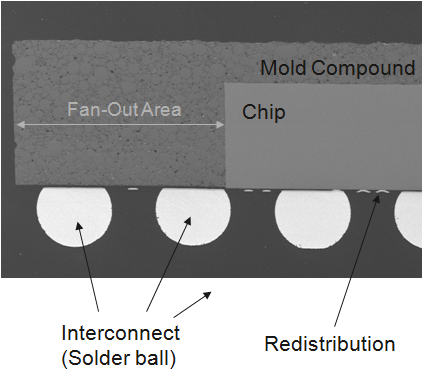
Embedded wafer level ball grid array (eWLB) is a packaging technology for integrated circuits. The package interconnects are applied on an artificial wafer made of silicon chips and a casting compound. eWLB is a further development of the classical wafer level ball grid array technology (WLB or WLP: wafer level package). The main driving force behind the eWLB technology was to allow fanout and more space for interconnect routing. All process steps for the generation of the package are performed on the wafer. This allows, in comparison to classical packaging technologies (e. g. ball grid array), the generation of very small and flat packages with excellent electrical and thermal performance at lowest cost. It is common for all WLB technologies, which are built on a silicon wafer, that the interconnects (typically solder balls) fit on the chip (so called fan-in design). Therefore only chips with a restricted number of interconnects can be packaged. The eWLB technology allows the ... [...More Info...] [...Related Items...] OR: [Wikipedia] [Google] [Baidu] |
Singulated
Singulation is a method by which an RFID reader identifies a tag with a specific serial number from a number of tags in its field. This is necessary because if multiple tags respond simultaneously to a query, they will jam each other. In a typical commercial application, such as scanning a bag of groceries, potentially hundreds of tags might be within range of the reader. When all the tags cooperate with the tag reader and follow the same anti-collision protocol, also called singulation protocol, Technovelgy"Problems With RFID" then the tag reader can read data from each and every tag without interference from the other tags. Collision avoidance Generally, a collision occurs when two entities require the same resource; for example, two ships with crossing courses in a narrows. In wireless technology, a collision occurs when two transmitters transmit at the same time with the same modulation scheme on the same frequency. In RFID technology, various strategies have been develop ... [...More Info...] [...Related Items...] OR: [Wikipedia] [Google] [Baidu] |
Infineon Technologies
Infineon Technologies AG is a German semiconductor manufacturer founded in 1999, when the semiconductor operations of the former parent company Siemens AG were spun off. Infineon has about 50,280 employees and is one of the ten largest semiconductor manufacturers worldwide. In fiscal year 2021, the company achieved sales of €11.06 billion. Infineon bought Cypress Semiconductor in April 2020. Markets Infineon markets semiconductors and systems for automotive, industrial, and multimarket sectors, as well as chip card and security products. Infineon has subsidiaries in the US in Milpitas, California, and in the Asia-Pacific region, in Singapore and Tokyo, Japan. Infineon has a number of facilities in Europe, one in Dresden. Infineon's high power segment is in Warstein, Germany; Villach and Graz in Austria; Cegléd in Hungary; and Italy. It also runs R&D centers in France, Singapore, Romania, Taiwan, UK, Ukraine and India, as well as fabrication units in Singapore, Malaysia, ... [...More Info...] [...Related Items...] OR: [Wikipedia] [Google] [Baidu] |
STMicroelectronics
STMicroelectronics N.V. commonly referred as ST or STMicro is a Dutch multinational corporation and technology company of French-Italian origin headquartered in Plan-les-Ouates near Geneva, Switzerland and listed on the French stock market. ST is the largest European semiconductor contract manufacturing and design company. The company resulted from the merger of two government-owned semiconductor companies in 1987: Thomson Semiconducteurs of France and SGS Microelettronica of Italy. History ST was formed in 1987 by the merger of two government-owned semiconductor companies: Italian SGS Microelettronica (where SGS stands for ''Società Generale Semiconduttori'', "Semiconductors' General Company"), and French Thomson Semiconducteurs, the semiconductor arm of Thomson. SGS Microelettronica originated in 1972 from a previous merger of two companies: * ATES (Aquila Tubi e Semiconduttori), a vacuum tube and semiconductor maker headquartered in L'Aquila, the regional capital of the r ... [...More Info...] [...Related Items...] OR: [Wikipedia] [Google] [Baidu] |
Automated Storage And Retrieval System
An automated storage and retrieval system (ASRS or AS/RS) consists of a variety of computer-controlled systems for automatically placing and retrieving loads from defined storage locations. Automated storage and retrieval systems (AS/RS) are typically used in applications where: * There is a very high volume of loads being moved into and out of storage * Storage density is important because of space constraints * No value is added in this process (no processing, only storage and transport) * Accuracy is critical because of potential expensive damages to the load An AS/RS can be used with standard loads as well as nonstandard loads, meaning that each standard load can fit in a uniformly-sized volume; for example, the film canisters in the image of the Defense Visual Information Center are each stored as part of the contents of the uniformly sized metal boxes, which are shown in the image. Standard loads simplify the handling of a request of an item. In addition, audits of the ac ... [...More Info...] [...Related Items...] OR: [Wikipedia] [Google] [Baidu] |
Molding (process)
Molding (American English) or moulding (British and Commonwealth English; see spelling differences) is the process of manufacturing by shaping liquid or pliable raw material using a rigid frame called a mold or matrix. This itself may have been made using a pattern or model of the final object. A mold or mould is a hollowed-out block that is filled with a liquid or pliable material such as plastic, glass, metal, or ceramic raw material. The liquid hardens or sets inside the mold, adopting its shape. A mold is a counterpart to a cast. The very common bi-valve molding process uses two molds, one for each half of the object. Articulated molds have multiple pieces that come together to form the complete mold, and then disassemble to release the finished casting; they are expensive, but necessary when the casting shape has complex overhangs. Piece-molding uses a number of different molds, each creating a section of a complicated object. This is generally only used for larger a ... [...More Info...] [...Related Items...] OR: [Wikipedia] [Google] [Baidu] |
Chip-scale Package
A chip scale package or chip-scale package (CSP) is a type of integrated circuit package. Originally, CSP was the acronym for ''chip-size packaging.'' Since only a few packages are chip size, the meaning of the acronym was adapted to ''chip-scale packaging''. According to IPC's standard J-STD-012, ''Implementation of Flip Chip and Chip Scale Technology'', in order to qualify as chip scale, the package must have an area no greater than 1.2 times that of the die and it must be a single-die, direct surface mountable package. Another criterion that is often applied to qualify these packages as CSPs is their ball pitch should be no more than 1 mm. The concept was first proposed by Junichi Kasai of Fujitsu and Gen Murakami of Hitachi Cable in 1993. The first concept demonstration however came from Mitsubishi Electric. The die may be mounted on an interposer upon which pads or balls are formed, like with flip chip ball grid array (BGA) packaging, or the pads may be etched or pr ... [...More Info...] [...Related Items...] OR: [Wikipedia] [Google] [Baidu] |
Ball Grid Array
A ball grid array (BGA) is a type of surface-mount packaging (a chip carrier) used for integrated circuits. BGA packages are used to permanently mount devices such as microprocessors. A BGA can provide more interconnection pins than can be put on a dual in-line or flat package. The whole bottom surface of the device can be used, instead of just the perimeter. The traces connecting the package's leads to the wires or balls which connect the die to package are also on average shorter than with a perimeter-only type, leading to better performance at high speeds. BGAs were introduced in the 1990s and became popular by 2001. Soldering of BGA devices requires precise control and is usually done by automated processes such as in computer-controlled automatic reflow ovens. Description The BGA is descended from the pin grid array (PGA), which is a package with one face covered (or partly covered) with pins in a grid pattern which, in operation, conduct electrical signals betwe ... [...More Info...] [...Related Items...] OR: [Wikipedia] [Google] [Baidu] |


