|
DDR-2
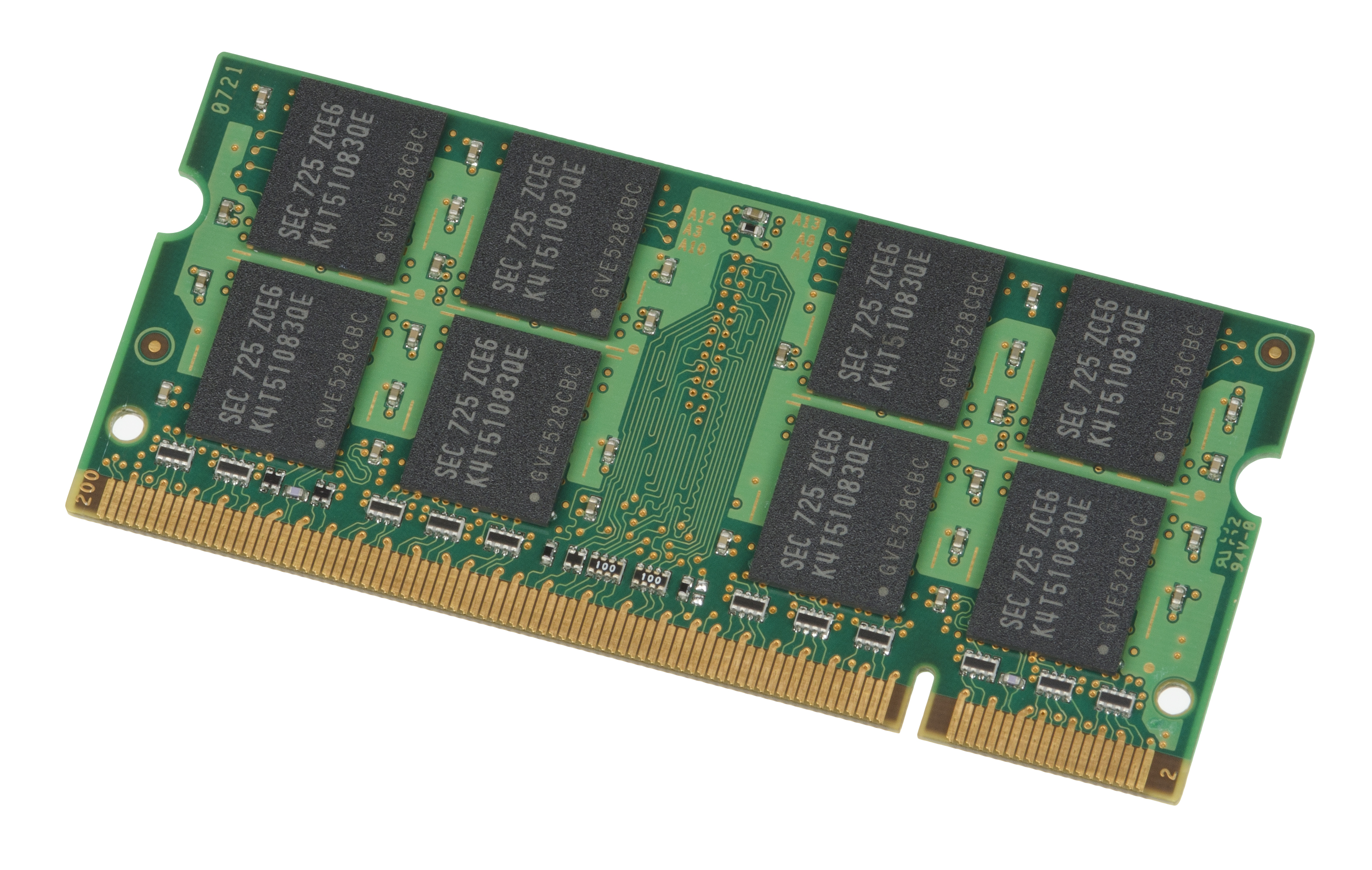
Double Data Rate 2 Synchronous Dynamic Random-Access Memory (DDR2 SDRAM) is a double data rate (DDR) synchronous dynamic random-access memory (SDRAM) interface. It superseded the original DDR SDRAM specification, and was itself superseded by DDR3 SDRAM (launched in 2007). DDR2 DIMMs are neither forward compatible with DDR3 nor backward compatible with DDR. In addition to double pumping the data bus as in DDR SDRAM (transferring data on the rising and falling edges of the bus clock signal), DDR2 allows higher bus speed and requires lower power by running the internal clock at half the speed of the data bus. The two factors combine to produce a total of four data transfers per internal clock cycle. Since the DDR2 internal clock runs at half the DDR external clock rate, DDR2 memory operating at the same external data bus clock rate as DDR results in DDR2 being able to provide the same bandwidth but with better latency. Alternatively, DDR2 memory operating at twice the external ... [...More Info...] [...Related Items...] OR: [Wikipedia] [Google] [Baidu] |
DDR SDRAM
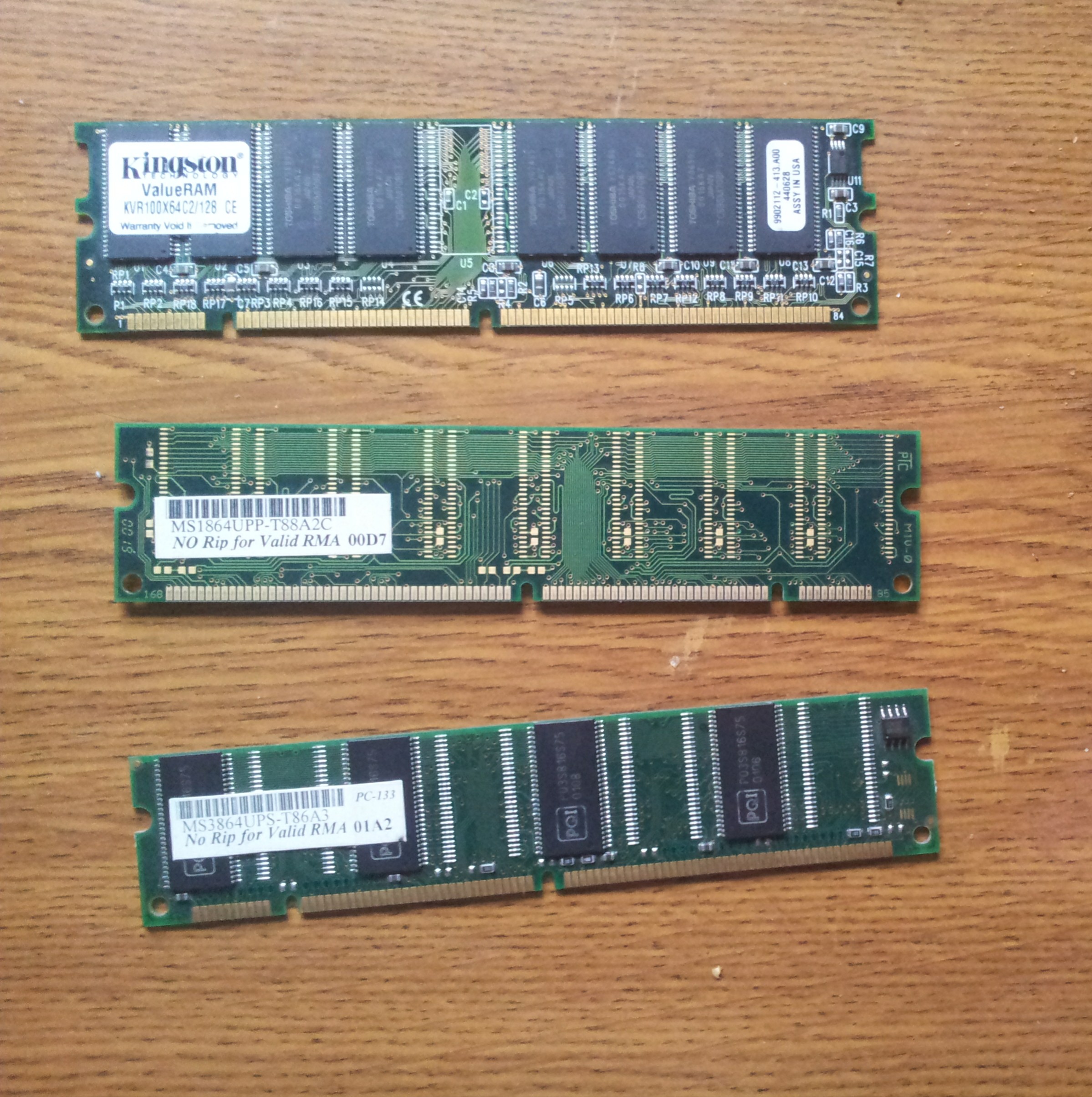
Double Data Rate Synchronous Dynamic Random-Access Memory (DDR SDRAM) is a double data rate (DDR) synchronous dynamic random-access memory (SDRAM) class of memory integrated circuits used in computers. DDR SDRAM, also retroactively called DDR1 SDRAM, has been superseded by DDR2 SDRAM, DDR3 SDRAM, DDR4 SDRAM and DDR5 SDRAM. None of its successors are forward or backward compatible with DDR1 SDRAM, meaning DDR2, DDR3, DDR4 and DDR5 memory modules will not work in DDR1-equipped motherboards, and vice versa. Compared to single data rate ( SDR) SDRAM, the DDR SDRAM interface makes higher transfer rates possible by more strict control of the timing of the electrical data and clock signals. Implementations often have to use schemes such as phase-locked loops and self-calibration to reach the required timing accuracy. The interface uses double pumping (transferring data on both the rising and falling edges of the clock signal) to double data bus bandwidth without a corresponding ... [...More Info...] [...Related Items...] OR: [Wikipedia] [Google] [Baidu] |
SO-DIMM
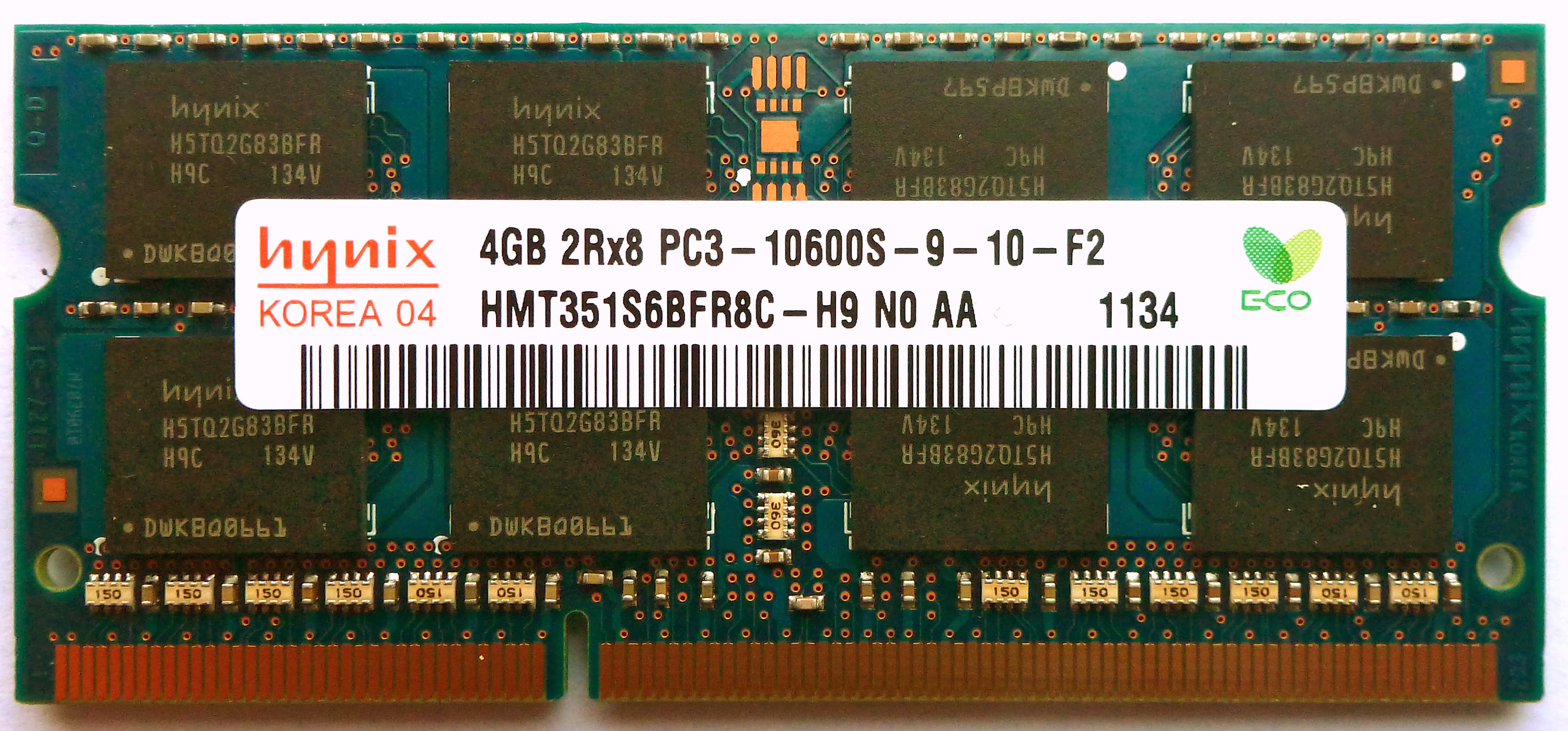
A DIMM () (Dual In-line Memory Module), commonly called a RAM stick, comprises a series of dynamic random-access memory integrated circuits. These memory modules are mounted on a printed circuit board and designed for use in personal computers, workstations, printers, and servers. They are the predominant method for adding memory into a computer system. The vast majority of DIMMs are standardized through JEDEC standards, although there are proprietary DIMMs. DIMMs come in a variety of speeds and sizes, but generally are one of two lengths - PC which are and laptop (SO-DIMM) which are about half the size at . History DIMMs (Dual In-line Memory Module) were a 1990s upgrade for SIMMs (Single In-line Memory Modules) as Intel P5-based Pentium processors began to gain market share. The Pentium had a 64-bit bus width, which would require SIMMs installed in matched pairs in order to populate the data bus. The processor would then access the two SIMMs in parallel. DIMMs were intr ... [...More Info...] [...Related Items...] OR: [Wikipedia] [Google] [Baidu] |
Double Data Rate
In computing, a computer bus operating with double data rate (DDR) transfers data on both the rising and falling edges of the clock signal. This is also known as double pumped, dual-pumped, and double transition. The term toggle mode is used in the context of NAND flash memory. Overview The simplest way to design a clocked electronic circuit is to make it perform one transfer per full cycle (rise and fall) of a clock signal. This, however, requires that the clock signal changes twice per transfer, while the data lines change at most once per transfer. When operating at a high bandwidth, signal integrity limitations constrain the clock frequency. By using both edges of the clock, the data signals operate with the same limiting frequency, thereby doubling the data transmission rate. This technique has been used for microprocessor front-side busses, Ultra-3 SCSI, expansion buses ( AGP, PCI-X), graphics memory (GDDR), main memory (both RDRAM and DDR1 through DDR5), and the ... [...More Info...] [...Related Items...] OR: [Wikipedia] [Google] [Baidu] |
DIMM
A DIMM () (Dual In-line Memory Module), commonly called a RAM stick, comprises a series of dynamic random-access memory integrated circuits. These memory modules are mounted on a printed circuit board and designed for use in personal computers, workstations, printers, and servers. They are the predominant method for adding memory into a computer system. The vast majority of DIMMs are standardized through JEDEC standards, although there are proprietary DIMMs. DIMMs come in a variety of speeds and sizes, but generally are one of two lengths - PC which are and laptop (SO-DIMM) which are about half the size at . History DIMMs (Dual In-line Memory Module) were a 1990s upgrade for SIMMs (Single In-line Memory Modules) as Intel P5-based Pentium processors began to gain market share. The Pentium had a 64-bit bus width, which would require SIMMs installed in matched pairs in order to populate the data bus. The processor would then access the two SIMMs in parallel. DIMMs were i ... [...More Info...] [...Related Items...] OR: [Wikipedia] [Google] [Baidu] |
Prefetch Buffer
Synchronous dynamic random-access memory (synchronous dynamic RAM or SDRAM) is any Dynamic RAM, DRAM where the operation of its external pin interface is coordinated by an externally supplied clock signal. DRAM integrated circuits (ICs) produced from the early 1970s to early 1990s used an ''asynchronous'' interface, in which input control signals have a direct effect on internal functions only delayed by the trip across its semiconductor pathways. SDRAM has a ''synchronous'' interface, whereby changes on control inputs are recognised after a rising edge of its clock input. In SDRAM families standardized by JEDEC, the clock signal controls the stepping of an internal finite-state machine that responds to incoming commands. These commands can be pipelined to improve performance, with previously started operations completing while new commands are received. The memory is divided into several equally sized but independent sections called ''Memory bank, banks'', allowing the device t ... [...More Info...] [...Related Items...] OR: [Wikipedia] [Google] [Baidu] |
Synchronous Dynamic Random-access Memory
Synchronous dynamic random-access memory (synchronous dynamic RAM or SDRAM) is any DRAM where the operation of its external pin interface is coordinated by an externally supplied clock signal. DRAM integrated circuits (ICs) produced from the early 1970s to early 1990s used an ''asynchronous'' interface, in which input control signals have a direct effect on internal functions only delayed by the trip across its semiconductor pathways. SDRAM has a ''synchronous'' interface, whereby changes on control inputs are recognised after a rising edge of its clock input. In SDRAM families standardized by JEDEC, the clock signal controls the stepping of an internal finite-state machine that responds to incoming commands. These commands can be pipelined to improve performance, with previously started operations completing while new commands are received. The memory is divided into several equally sized but independent sections called ''banks'', allowing the device to operate on a memory a ... [...More Info...] [...Related Items...] OR: [Wikipedia] [Google] [Baidu] |
SDR SDRAM
Synchronous dynamic random-access memory (synchronous dynamic RAM or SDRAM) is any DRAM where the operation of its external pin interface is coordinated by an externally supplied clock signal. DRAM integrated circuits (ICs) produced from the early 1970s to early 1990s used an ''asynchronous'' interface, in which input control signals have a direct effect on internal functions only delayed by the trip across its semiconductor pathways. SDRAM has a ''synchronous'' interface, whereby changes on control inputs are recognised after a rising edge of its clock input. In SDRAM families standardized by JEDEC, the clock signal controls the stepping of an internal finite-state machine that responds to incoming commands. These commands can be pipelined to improve performance, with previously started operations completing while new commands are received. The memory is divided into several equally sized but independent sections called ''banks'', allowing the device to operate on a memory acce ... [...More Info...] [...Related Items...] OR: [Wikipedia] [Google] [Baidu] |
Memory Latency
''Memory latency'' is the time (the latency) between initiating a request for a byte or word in memory until it is retrieved by a processor. If the data are not in the processor's cache, it takes longer to obtain them, as the processor will have to communicate with the external memory cells. Latency is therefore a fundamental measure of the speed of memory: the less the latency, the faster the reading operation. Latency should not be confused with memory bandwidth, which measures the throughput of memory. Latency can be expressed in clock cycles or in time measured in nanoseconds. Over time, memory latencies expressed in clock cycles have been fairly stable, but they have improved in time.Crucial Technology, "Speed ''vs.'' Latency: Why CAS latency isn't an accurate measure of memory performance/ref> See also * Burst mode (computing) * CAS latency * Multi-channel memory architecture * Interleaved memory * SDRAM burst ordering * SDRAM latency Memory timings or RAM timings descr ... [...More Info...] [...Related Items...] OR: [Wikipedia] [Google] [Baidu] |
Ball Grid Array
A ball grid array (BGA) is a type of surface-mount packaging (a chip carrier) used for integrated circuits. BGA packages are used to permanently mount devices such as microprocessors. A BGA can provide more interconnection pins than can be put on a dual in-line or flat package. The whole bottom surface of the device can be used, instead of just the perimeter. The traces connecting the package's leads to the wires or balls which connect the die to package are also on average shorter than with a perimeter-only type, leading to better performance at high speeds. BGAs were introduced in the 1990s and became popular by 2001. Soldering of BGA devices requires precise control and is usually done by automated processes such as in computer-controlled automatic reflow ovens. Description The BGA is descended from the pin grid array (PGA), which is a package with one face covered (or partly covered) with pins in a grid pattern which, in operation, conduct electrical signals betwe ... [...More Info...] [...Related Items...] OR: [Wikipedia] [Google] [Baidu] |
TSSOP
The Thin Shrink Small Outline Package (TSSOP) is a rectangular surface mount plastic integrated circuit (IC) package with gull-wing leads. Application They are suited for applications requiring 1 mm or less mounted height and are commonly used in analog and operation amplifiers, controllers and Drivers, Logic, Memory, and RF/Wireless, Disk drives, video/audio and consumer electronics. Physical properties The Thin shrink small outline package has a smaller body and smaller lead pitch than the standard SOIC package. It is also smaller and thinner than a TSOP with the same lead count. Body widths are 3.0 mm, 4.4 mm and 6.1 mm. The lead counts range from 8 to 80 pins. The lead pitches are 0.5 or 0.65 mm. Exposed Pad Some TSSOP packages have an exposed pad. This is a rectangular metal pad on the bottom side of the package. The exposed pad will be soldered on the pcb to transfer heat from the package to the pcb. In most applications, the exposed pad ... [...More Info...] [...Related Items...] OR: [Wikipedia] [Google] [Baidu] |
Samsung
The Samsung Group (or simply Samsung) ( ko, 삼성 ) is a South Korean multinational manufacturing conglomerate headquartered in Samsung Town, Seoul, South Korea. It comprises numerous affiliated businesses, most of them united under the ''Samsung'' brand, and is the largest South Korean (business conglomerate). Samsung has the eighth highest global brand value. Samsung was founded by Lee Byung-chul in 1938 as a trading company. Over the next three decades, the group diversified into areas including food processing, textiles, insurance, securities, and retail. Samsung entered the electronics industry in the late 1960s and the construction and shipbuilding industries in the mid-1970s; these areas would drive its subsequent growth. Following Lee's death in 1987, Samsung was separated into five business groups – Samsung Group, Shinsegae Group, CJ Group and Hansol Group, and JoongAng Group. Notable Samsung industrial affiliates include Samsung Electronics (the wor ... [...More Info...] [...Related Items...] OR: [Wikipedia] [Google] [Baidu] |

.jpg)


