|
Plasmonics
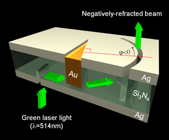
Plasmonics or nanoplasmonics refers to the generation, detection, and manipulation of signals at optical frequencies along metal-dielectric interfaces in the nanometer scale. Inspired by photonics, plasmonics follows the trend of miniaturizing optical devices (see also nanophotonics), and finds applications in sensing, microscopy, optical communications, and bio-photonics. Principles Plasmonics typically utilizes Surface plasmon polariton, surface plasmon polaritons (SPPs), that are coherent electron oscillations travelling together with an Electromagnetic radiation, electromagnetic wave along the interface between a dielectric (e.g. glass, air) and a metal (e.g. silver, gold). The SPP modes are strongly confined to their supporting interface, giving rise to strong light-matter interactions. In particular, the electron gas in the metal oscillates with the electro-magnetic wave. Because the moving electrons are scattered, ohmic losses in plasmonic signals are generally large, wh ... [...More Info...] [...Related Items...] OR: [Wikipedia] [Google] [Baidu] |
Surface Plasmon Polariton
Surface plasmon polaritons (SPPs) are electromagnetic waves that travel along a metal–dielectric or metal–air interface, practically in the infrared or visible spectrum, visible-frequency. The term "surface plasmon polariton" explains that the wave involves both charge motion in the metal ("surface plasmon") and electromagnetic waves in the air or dielectric ("polariton"). They are a type of surface wave, guided along the interface in much the same way that light can be guided by an optical fiber. SPPs have a shorter wavelength than light in vacuum at the same frequency (photons). Hence, SPPs can have a higher Photon#Relativistic energy and momentum , momentum and field intensity, local field intensity. Perpendicular to the interface, they have subwavelength-scale confinement. An SPP will propagate along the interface until its energy is lost either to absorption in the metal or scattering into other directions (such as into free space). Application of SPPs enables subwavelen ... [...More Info...] [...Related Items...] OR: [Wikipedia] [Google] [Baidu] |
Plasmonic Waveguide Device Visible Freq
In physics, a plasmon is a quantum of plasma oscillation. Just as light (an optical oscillation) consists of photons, the plasma oscillation consists of plasmons. The plasmon can be considered as a quasiparticle since it arises from the quantization of plasma oscillations, just like phonons are quantizations of mechanical vibrations. Thus, plasmons are collective (a discrete number) oscillations of the free electron gas density. For example, at optical frequencies, plasmons can couple with a photon to create another quasiparticle called a plasmon polariton. The field of study and manipulation of plasmons is called plasmonics. Derivation The plasmon was initially proposed in 1952 by David Pines and David Bohm and was shown to arise from a Hamiltonian for the long-range electron-electron correlations. Since plasmons are the quantization of classical plasma oscillations, most of their properties can be derived directly from Maxwell's equations. Explanation Plasmons can b ... [...More Info...] [...Related Items...] OR: [Wikipedia] [Google] [Baidu] |
Localized Surface Plasmon
A localized surface plasmon (LSP) is the result of the confinement of a surface plasmon in a nanoparticle of size comparable to or smaller than the wavelength of light used to excite the plasmon. When a small spherical metallic nanoparticle is irradiated by light, the oscillating electric field causes the conduction electrons to oscillate coherently. When the electron cloud is displaced relative to its original position, a restoring force arises from Coulombic attraction between electrons and nuclei. This force causes the electron cloud to oscillate. The oscillation frequency is determined by the density of electrons, the effective electron mass, and the size and shape of the charge distribution. The LSP has two important effects: electric fields near the particle's surface are greatly enhanced and the particle's optical absorption has a maximum at the plasmon resonant frequency. Surface plasmon resonance can also be tuned based on the shape of the nanoparticle. The plasmon frequenc ... [...More Info...] [...Related Items...] OR: [Wikipedia] [Google] [Baidu] |
Nanophotonics
Nanophotonics or nano-optics is the study of the behavior of light on the nanometer scale, and of the interaction of nanometer-scale objects with light. It is a branch of optics, optical engineering, electrical engineering, and nanotechnology. It often involves dielectric structures such as nanoantennas, or metallic components, which can transport and focus light via surface plasmon polaritons. The term "nano-optics", just like the term "optics", usually refers to situations involving ultraviolet, visible, and near-infrared light (free-space wavelengths from 300 to 1200 nanometers). Background Normal optical components, like lenses and microscopes, generally cannot normally focus light to nanometer (deep subwavelength) scales, because of the diffraction limit ( Rayleigh criterion). Nevertheless, it is possible to squeeze light into a nanometer scale using other techniques like, for example, surface plasmons, localized surface plasmons around nanoscale metal objects, and ... [...More Info...] [...Related Items...] OR: [Wikipedia] [Google] [Baidu] |
Bragg Mirror
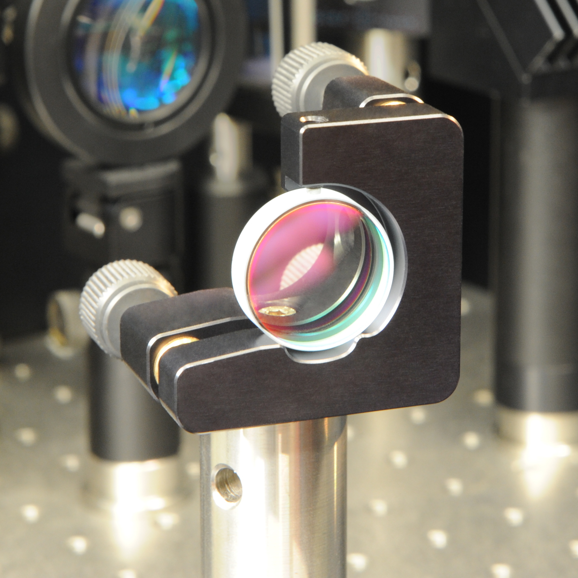
A dielectric mirror, also known as a Bragg mirror, is a type of mirror composed of multiple thin layers of dielectric material, typically deposited on a substrate of glass or some other optical material. By careful choice of the type and thickness of the dielectric layers, one can design an optical coating with specified reflectivity at different wavelengths of light. Dielectric mirrors are also used to produce ultra-high reflectivity mirrors: values of 99.999% or better over a narrow range of wavelengths can be produced using special techniques. Alternatively, they can be made to reflect a broad spectrum of light, such as the entire visible range or the spectrum of the Ti-sapphire laser. Dielectric mirrors are very common in optics experiments, due to improved techniques that allow inexpensive manufacture of high-quality mirrors. Examples of their applications include laser cavity end mirrors, hot and cold mirrors, thin-film beamsplitters, high damage threshold mirrors, an ... [...More Info...] [...Related Items...] OR: [Wikipedia] [Google] [Baidu] |
Science (journal)
''Science'' is the peer review, peer-reviewed academic journal of the American Association for the Advancement of Science (AAAS) and one of the world's top academic journals. It was first published in 1880, is currently circulated weekly and has a subscriber base of around 130,000. Because institutional subscriptions and online access serve a larger audience, its estimated readership is over 400,000 people. ''Science'' is based in Washington, D.C., United States, with a second office in Cambridge, UK. Contents The major focus of the journal is publishing important original scientific research and research reviews, but ''Science'' also publishes science-related news, opinions on science policy and other matters of interest to scientists and others who are concerned with the wide implications of science and technology. Unlike most scientific journals, which focus on a specific field, ''Science'' and its rival ''Nature (journal), Nature'' cover the full range of List of academ ... [...More Info...] [...Related Items...] OR: [Wikipedia] [Google] [Baidu] |
Optical Materials Express
''Optical Materials Express'' is a monthly peer-reviewed scientific journal published by Optica. It covers advances in and applications of optical materials, including but not limited to nonlinear optical materials, laser media, nanomaterials, metamaterials and biomaterials. Its editor-in-chief is Andrea Alù (City University of New York). The founding editor-in-chief was David J. Hagan. According to the ''Journal Citation Reports'', the journal has a 2023 impact factor The impact factor (IF) or journal impact factor (JIF) of an academic journal is a type of journal ranking. Journals with higher impact factor values are considered more prestigious or important within their field. The Impact Factor of a journa ... of 2.8. References External links * Optics journals Materials science journals English-language journals Monthly journals Academic journals established in 2011 Optica (society) academic journals {{materials-journal-stub ... [...More Info...] [...Related Items...] OR: [Wikipedia] [Google] [Baidu] |
Graphene
Graphene () is a carbon allotrope consisting of a Single-layer materials, single layer of atoms arranged in a hexagonal lattice, honeycomb planar nanostructure. The name "graphene" is derived from "graphite" and the suffix -ene, indicating the presence of double bonds within the carbon structure. Graphene is known for its exceptionally high Ultimate tensile strength, tensile strength, Electrical resistivity and conductivity, electrical conductivity, Transparency and translucency, transparency, and being the thinnest two-dimensional material in the world. Despite the nearly transparent nature of a single graphene sheet, graphite (formed from stacked layers of graphene) appears black because it absorbs all visible light wavelengths. On a microscopic scale, graphene is the strongest material ever measured. The existence of graphene was first theorized in 1947 by P. R. Wallace, Philip R. Wallace during his research on graphite's electronic properties, while the term ''graphen ... [...More Info...] [...Related Items...] OR: [Wikipedia] [Google] [Baidu] |
Nanoscale (journal)
''Nanoscale'' is a peer-reviewed scientific journal covering experimental and theoretical research in all areas of nanotechnology and nanoscience. It is published by the Royal Society of Chemistry. According to the ''Journal Citation Reports'', the journal has a 2021 impact factor The impact factor (IF) or journal impact factor (JIF) of an academic journal is a type of journal ranking. Journals with higher impact factor values are considered more prestigious or important within their field. The Impact Factor of a journa ... of 8.307. References External links * Royal Society of Chemistry academic journals Biweekly journals Academic journals established in 2009 Nanotechnology journals English-language journals {{nano-journal-stub ... [...More Info...] [...Related Items...] OR: [Wikipedia] [Google] [Baidu] |
Photonics (journal)
This is a list of academic journals published by MDPI. As of September 2022, MDPI publishes 399 peer-reviewed academic journals and nine conference journals. {, class="wikitable sortable" , +List of MDPI journals !Journal name !Subject !Established !ISSN , - , ''Acoustics'' , Engineering , 2019 , 2624-599X , - , ''Actuators'' , Engineering , 2012 , 2076-0825 , - , ''Administrative Sciences'' , Business , 2011 , 2076-3387 , - , ''Adolescents'' , Health , 2021 , 2673-7051 , - , ''Advances in Respiratory Medicine'' (formerly ''Pneumonologia i Alergologia Polska)'' , Health , , 2451-4934 , - , ''Aerospace'' , Engineering , 2014 , 2226-4310 , - , ''Agriculture'' , Agriculture , 2011 , 2077-0472 , - , ''AgriEngineering'' , Agriculture , 2019 , 2624-7402 , - , ''Agronomy'' , Agriculture , 2011 , 2073-4395 , - , ''AI'' , Computers , 2020 , 2673-2688 , - , ''Algorithms'' , Mathematics , 2008 , 1999-4893 , - , ''Allergies'' , Medicine , 2021 , 2313-5786 , - , ''Alloys'' , Engineering ... [...More Info...] [...Related Items...] OR: [Wikipedia] [Google] [Baidu] |
CMOS
Complementary metal–oxide–semiconductor (CMOS, pronounced "sea-moss ", , ) is a type of MOSFET, metal–oxide–semiconductor field-effect transistor (MOSFET) semiconductor device fabrication, fabrication process that uses complementary and symmetrical pairs of p-type semiconductor, p-type and n-type semiconductor, n-type MOSFETs for logic functions. CMOS technology is used for constructing integrated circuit (IC) chips, including microprocessors, microcontrollers, memory chips (including Nonvolatile BIOS memory, CMOS BIOS), and other digital logic circuits. CMOS technology is also used for analog circuits such as image sensors (CMOS sensors), data conversion, data converters, RF circuits (RF CMOS), and highly integrated transceivers for many types of communication. In 1948, Bardeen and Brattain patented an insulated-gate transistor (IGFET) with an inversion layer. Bardeen's concept forms the basis of CMOS technology today. The CMOS process was presented by Fairchild Semico ... [...More Info...] [...Related Items...] OR: [Wikipedia] [Google] [Baidu] |


