|
Beyond CMOS
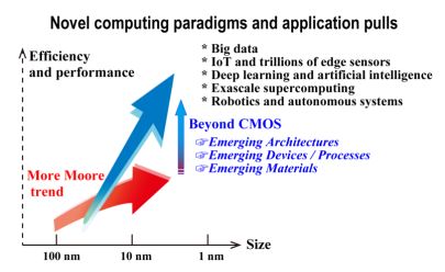
Beyond CMOS refers to the possible future digital logic technologies beyond the CMOS scaling limits which limits device density and speeds due to heating effects. ''Beyond CMOS'' is the name of one of the 7 focus groups in ITRS 2.0 (2013) and in its successor, the International Roadmap for Devices and Systems. CPUs using CMOS were released from 1986 (e.g. 12 MHz Intel 80386). As CMOS transistor dimensions were shrunk the clock speeds also increased. Since about 2004 CMOS CPU clock speeds have leveled off at about 3.5 GHz. CMOS devices sizes continue to shrink – see Intel tick–tock and ITRS : * 22 nanometer Ivy Bridge in 2012 * first 14 nanometer processors shipped in Q4 2014. * In May 2015, Samsung Electronics showed a 300 mm wafer of 10 nanometer FinFET chips. It is not yet clear if CMOS transistors will still work below 3 nm. See 3 nanometer. Comparisons of technology About 2010 the Nanoelectronic Research Initiative (NRI) studied various ... [...More Info...] [...Related Items...] OR: [Wikipedia] [Google] [Baidu] |
Digital Logic
A logic gate is an idealized or physical device implementing a Boolean function, a logical operation performed on one or more Binary number, binary inputs that produces a single binary output. Depending on the context, the term may refer to an ideal logic gate, one that has for instance zero rise time and unlimited fan-out, or it may refer to a non-ideal physical device (see Ideal and real op-amps for comparison). Logic gates are primarily implemented using diodes or transistors acting as switch#Electronic switches, electronic switches, but can also be constructed using vacuum tubes, electromagnetic relays (relay logic), fluidic logic, pneumatics#Pneumatic logic, pneumatic logic, optics, molecular logic gate, molecules, or even analytical engine, mechanical elements. Now, most logic gates are made from MOSFETs (metal–oxide–semiconductor field-effect transistors). With amplification, logic gates can be cascaded in the same way that Boolean functions can be composed, allowing t ... [...More Info...] [...Related Items...] OR: [Wikipedia] [Google] [Baidu] |
Spintronic
Spintronics (a portmanteau meaning spin transport electronics), also known as spin electronics, is the study of the intrinsic spin of the electron and its associated magnetic moment, in addition to its fundamental electronic charge, in solid-state devices. The field of spintronics concerns spin-charge coupling in metallic systems; the analogous effects in insulators fall into the field of multiferroics. Spintronics fundamentally differs from traditional electronics in that, in addition to charge state, electron spins are exploited as a further degree of freedom, with implications in the efficiency of data storage and transfer. Spintronic systems are most often realised in dilute magnetic semiconductors (DMS) and Heusler alloys and are of particular interest in the field of quantum computing and neuromorphic computing. History Spintronics emerged from discoveries in the 1980s concerning spin-dependent electron transport phenomena in solid-state devices. This includes the observ ... [...More Info...] [...Related Items...] OR: [Wikipedia] [Google] [Baidu] |
Polariton Superfluid
Polariton superfluid is predicted to be a state of the exciton-polaritons system that combines the characteristics of lasers with those of excellent electrical conductors. Researchers look for this state in a solid state optical microcavity coupled with quantum well excitons. The idea is to create an ensemble of particles known as exciton-polaritons and trap them. Wave behavior in this state results in a light beam similar to that from a laser but possibly more energy efficient. Unlike traditional superfluids that need temperatures of approximately ~4 K, the polariton superfluid could in principle be stable at much higher temperatures, and might soon be demonstrable at room temperature. Evidence for polariton superfluidity was reported in by Alberto Amo and coworkers, based on the suppressed scattering of the polaritons during their motion. Although several other researchers are working in the same field, the terminology and conclusions are not completely shared by the differe ... [...More Info...] [...Related Items...] OR: [Wikipedia] [Google] [Baidu] |
Topological Insulator
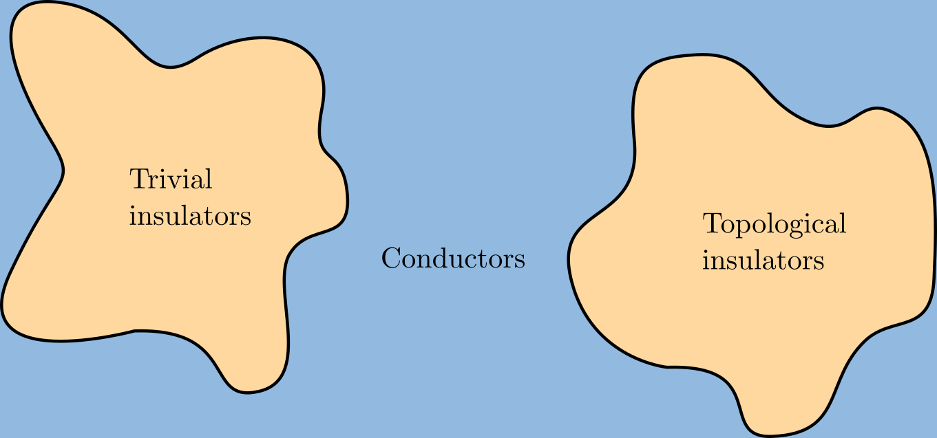
A topological insulator is a material whose interior behaves as an electrical insulator while its surface behaves as an electrical conductor, meaning that electrons can only move along the surface of the material. A topological insulator is an insulator for the same reason a "trivial" (ordinary) insulator is: there exists an energy gap between the valence and conduction bands of the material. But in a topological insulator, these bands are, in an informal sense, "twisted", relative to a trivial insulator. The topological insulator cannot be continuously transformed into a trivial one without untwisting the bands, which closes the band gap and creates a conducting state. Thus, due to the continuity of the underlying field, the border of a topological insulator with a trivial insulator (including vacuum, which is topologically trivial) is forced to support a conducting state. Since this results from a global property of the topological insulator's band structure, local (symmetry- ... [...More Info...] [...Related Items...] OR: [Wikipedia] [Google] [Baidu] |
ARC Centre Of Excellence In Future Low-Energy Electronics Technologies
ARC may refer to: Business * Aircraft Radio Corporation, a major avionics manufacturer from the 1920s to the '50s * Airlines Reporting Corporation, an airline-owned company that provides ticket distribution, reporting, and settlement services * Airport Regions Conference, a European organization of major airports * Amalgamated Roadstone Corporation, a British stone quarrying company * American Record Company (1904–1908, re-activated 1979), one of two United States record labels by this name * American Record Corporation (1929–1938), a United States record label also known as American Record Company * ARC (American Recording Company) (1978-present), a vanity label for Earth, Wind & Fire * ARC Document Solutions, a company based in California, formerly American Reprographics Company * Amey Roadstone Construction, a former British construction company * Aqaba Railway Corporation, a freight railway in Jordan * ARC/Architectural Resources Cambridge, Inc., Cambridge, Massachuset ... [...More Info...] [...Related Items...] OR: [Wikipedia] [Google] [Baidu] |
Spintronics
Spintronics (a portmanteau meaning spin transport electronics), also known as spin electronics, is the study of the intrinsic spin of the electron and its associated magnetic moment, in addition to its fundamental electronic charge, in solid-state devices. The field of spintronics concerns spin-charge coupling in metallic systems; the analogous effects in insulators fall into the field of multiferroics. Spintronics fundamentally differs from traditional electronics in that, in addition to charge state, electron spins are exploited as a further degree of freedom, with implications in the efficiency of data storage and transfer. Spintronic systems are most often realised in dilute magnetic semiconductors (DMS) and Heusler alloys and are of particular interest in the field of quantum computing and neuromorphic computing. History Spintronics emerged from discoveries in the 1980s concerning spin-dependent electron transport phenomena in solid-state devices. This includes the observa ... [...More Info...] [...Related Items...] OR: [Wikipedia] [Google] [Baidu] |
Molecular Electronics
Molecular electronics is the study and application of molecular building blocks for the fabrication of electronic components. It is an interdisciplinary area that spans physics, chemistry, and materials science. The unifying feature is use of molecular building blocks to fabricate electronic components. Due to the prospect of size reduction in electronics offered by molecular-level control of properties, molecular electronics has generated much excitement. It provides a potential means to extend Moore's Law beyond the foreseen limits of small-scale conventional silicon integrated circuits. Molecular scale electronics Molecular scale electronics, also called single-molecule electronics, is a branch of nanotechnology that uses single molecules, or nanoscale collections of single molecules, as electronic components. Because single molecules constitute the smallest stable structures possible, this miniaturization is the ultimate goal for shrinking electrical circuits. Convention ... [...More Info...] [...Related Items...] OR: [Wikipedia] [Google] [Baidu] |
Graphene Nanoribbons
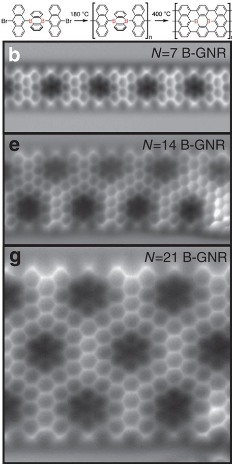
Graphene nanoribbons (GNRs, also called nano-graphene ribbons or nano-graphite ribbons) are strips of graphene with width less than 100 nm. Graphene ribbons were introduced as a theoretical model by Mitsutaka Fujita and coauthors to examine the edge and nanoscale size effect in graphene. Production Nanotomy Large quantities of width-controlled GNRs can be produced via graphite nanotomy, where applying a sharp diamond knife on graphite produces graphite nanoblocks, which can then be exfoliated to produce GNRs as shown by Vikas Berry. GNRs can also be produced by "unzipping" or axially cutting nanotubes. In one such method multi-walled carbon nanotubes were unzipped in solution by action of potassium permanganate and sulfuric acid. In another method GNRs were produced by plasma etching of nanotubes partly embedded in a polymer film. More recently, graphene nanoribbons were grown onto silicon carbide (SiC) substrates using ion implantation followed by vacuum or laser a ... [...More Info...] [...Related Items...] OR: [Wikipedia] [Google] [Baidu] |
Carbon Nanotube Field-effect Transistor
A carbon nanotube field-effect transistor (CNTFET) is a field-effect transistor that utilizes a single carbon nanotube or an array of carbon nanotubes as the channel material instead of bulk silicon in the traditional MOSFET structure. First demonstrated in 1998, there have been major developments in CNTFETs since. Introduction and background According to Moore's law, the dimensions of individual devices in an integrated circuit have been decreased by a factor of approximately two every two years. This scaling down of devices has been the driving force in technological advances since the late 20th century. However, as noted by ITRS 2009 edition, further scaling down has faced serious limits related to fabrication technology and device performances as the critical dimension shrunk down to sub-22 nm range. The limits involve electron tunneling through short channels and thin insulator films, the associated leakage currents, passive power dissipation, short channel effects, and v ... [...More Info...] [...Related Items...] OR: [Wikipedia] [Google] [Baidu] |
Indium Antimonide
Indium antimonide (InSb) is a crystalline compound made from the elements indium (In) and antimony (Sb). It is a narrow- gap semiconductor material from the III- V group used in infrared detectors, including thermal imaging cameras, FLIR systems, infrared homing missile guidance systems, and in infrared astronomy. The indium antimonide detectors are sensitive between 1–5 μm wavelengths. Indium antimonide was a very common detector in the old, single-detector mechanically scanned thermal imaging systems. Another application is as a terahertz radiation source as it is a strong photo-Dember emitter. History The intermetallic compound was first reported by Liu and Peretti in 1951, who gave its homogeneity range, structure type, and lattice constant. Polycrystalline ingots of InSb were prepared by Heinrich Welker in 1952, although they were not very pure by today's semiconductor standards. Welker was interested in systematically studying the semiconducting properties of t ... [...More Info...] [...Related Items...] OR: [Wikipedia] [Google] [Baidu] |
Tunnel Field-effect Transistor
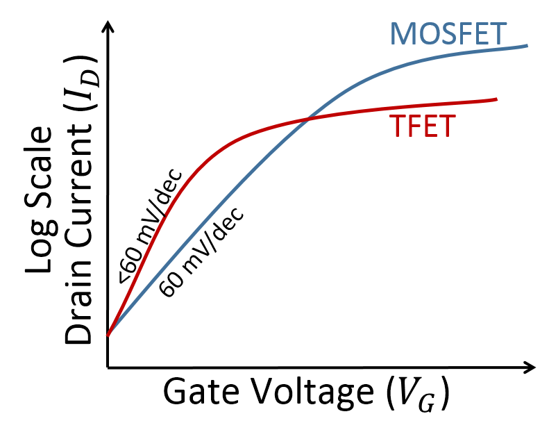
The tunnel field-effect transistor (TFET) is an experimental type of transistor. Even though its structure is very similar to a metal-oxide-semiconductor field-effect transistor ( MOSFET), the fundamental switching mechanism differs, making this device a promising candidate for low power electronics. TFETs switch by modulating quantum tunneling through a barrier instead of modulating thermionic emission over a barrier as in traditional MOSFETs. Because of this, TFETs are not limited by the thermal Maxwell–Boltzmann tail of carriers, which limits MOSFET drain current subthreshold swing to about 60 mV/decade of current at room temperature. TFET studies can be traced back to Stuetzer who in 1952 published first investigations of a transistor containing the basic elements of the TFET, a gated p-n junction. The reported surface conductivity control was, however, not related to tunneling. The first TFET was reported in 1965. Joerg Appenzeller and his colleagues at IBM were the first ... [...More Info...] [...Related Items...] OR: [Wikipedia] [Google] [Baidu] |
Tunnel Junction
In electronics/spintronics, a tunnel junction is a barrier, such as a thin insulating layer or electric potential, between two electrically conducting materials. Electrons (or quasiparticles) pass through the barrier by the process of quantum tunnelling. Classically, the electron has zero probability of passing through the barrier. However, according to quantum mechanics, the electron has a non-zero wave amplitude in the barrier, and hence it has some probability of passing through the barrier. Tunnel junctions serve a variety of different purposes. Multijunction photovoltaic cell In multijunction photovoltaic cells, tunnel junctions form the connections between consecutive p-n junctions. They function as an ohmic contact, ohmic electrical contact in the middle of a semiconductor device. Magnetic tunnel junction In magnetic tunnel junctions, electrons tunnel through a thin insulating barrier from one magnetic material to another. This can serve as a basis for a magnetic detector. ... [...More Info...] [...Related Items...] OR: [Wikipedia] [Google] [Baidu] |


