|
Bismuth Telluride
Bismuth telluride (Bi2Te3) is a gray powder that is a compound of bismuth and tellurium also known as bismuth(III) telluride. It is a semiconductor, which, when alloyed with antimony or selenium, is an efficient thermoelectric material for refrigeration or portable power generation. Bi2Te3 is a topological insulator, and thus exhibits thickness-dependent physical properties. Properties as a thermoelectric material Bismuth telluride is a narrow-gap layered semiconductor with a trigonal unit cell. The valence and conduction band structure can be described as a many-ellipsoidal model with 6 constant-energy ellipsoids that are centered on the reflection planes. Bi2Te3 cleaves easily along the trigonal axis due to Van der Waals bonding between neighboring tellurium atoms. Due to this, bismuth-telluride-based materials used for power generation or cooling applications must be polycrystalline. Furthermore, the Seebeck coefficient of bulk Bi2Te3 becomes compensated around room temperatur ... [...More Info...] [...Related Items...] OR: [Wikipedia] [Google] [Baidu] |
Crystal Twinning
Crystal twinning occurs when two or more adjacent crystals of the same mineral are oriented so that they share some of the same crystal lattice points in a symmetrical manner. The result is an intergrowth of two separate crystals that are tightly bonded to each other. The surface along which the lattice points are shared in twinned crystals is called a composition surface or twin plane. Crystallographers classify twinned crystals by a number of twin laws. These twin laws are specific to the crystal structure. The type of twinning can be a diagnostic tool in mineral identification. Deformation twinning, in which twinning develops in a crystal in response to a shear stress, is an important mechanism for permanent shape changes in a crystal.Courtney, Thomas H. (2000) ''Mechanical Behavior of Materials'', 2nd ed. McGraw Hill. Definition Twinning is a form of symmetrical intergrowth between two or more adjacent crystals of the same mineral. It differs from the ordinary random ... [...More Info...] [...Related Items...] OR: [Wikipedia] [Google] [Baidu] |
Band Gap
In solid-state physics, a band gap, also called an energy gap, is an energy range in a solid where no electronic states can exist. In graphs of the electronic band structure of solids, the band gap generally refers to the energy difference (in electron volts) between the top of the valence band and the bottom of the conduction band in insulators and semiconductors. It is the energy required to promote a valence electron bound to an atom to become a conduction electron, which is free to move within the crystal lattice and serve as a charge carrier to conduct electric current. It is closely related to the HOMO/LUMO gap in chemistry. If the valence band is completely full and the conduction band is completely empty, then electrons cannot move within the solid because there are no available states. If the electrons are not free to move within the crystal lattice, then there is no generated current due to no net charge carrier mobility. However, if some electrons transfer ... [...More Info...] [...Related Items...] OR: [Wikipedia] [Google] [Baidu] |
Acetone
Acetone (2-propanone or dimethyl ketone), is an organic compound with the formula . It is the simplest and smallest ketone (). It is a colorless, highly volatile and flammable liquid with a characteristic pungent odour. Acetone is miscible with water and serves as an important organic solvent in its own right, in industry, home, and laboratory. About 6.7 million tonnes were produced worldwide in 2010, mainly for use as a solvent and production of methyl methacrylate (and from that PMMA) as well as bisphenol A.Acetone World Petrochemicals report, January 2010Stylianos Sifniades, Alan B. Levy, "Acetone" in Ullmann's Encyclopedia of Industrial Chemistry, Wiley-VCH, Weinheim, 2005. It is a common building block in |
Atomic Force Microscopy
Atomic force microscopy (AFM) or scanning force microscopy (SFM) is a very-high-resolution type of scanning probe microscopy (SPM), with demonstrated resolution on the order of fractions of a nanometer, more than 1000 times better than the optical diffraction limit. Overview Atomic force microscopy (AFM) is a type of scanning probe microscopy (SPM), with demonstrated resolution on the order of fractions of a nanometer, more than 1000 times better than the optical diffraction limit. The information is gathered by "feeling" or "touching" the surface with a mechanical probe. Piezoelectric elements that facilitate tiny but accurate and precise movements on (electronic) command enable precise scanning. Despite the name, the Atomic Force Microscope does not use the Nuclear force. Abilities The AFM has three major abilities: force measurement, topographic imaging, and manipulation. In force measurement, AFMs can be used to measure the forces between the probe and the sample as ... [...More Info...] [...Related Items...] OR: [Wikipedia] [Google] [Baidu] |
Substrate (materials Science)
Substrate is a term used in materials science and engineering to describe the base material on which processing is conducted. This surface could be used to produce new film or layers of material such as deposited coatings. It could be the base to which paint, adhesives, or adhesive tape is bonded. A typical substrate might be rigid such as metal, concrete, or glass, onto which a coating might be deposited. Flexible substrates are also used. With all coating processes, the condition of the surface of the substrate can strongly affect the bond of subsequent layers. This can include cleanliness, smoothness, surface energy, moisture, etc. Some substrates are anisotropic with surface properties being different depending on the direction: examples include wood and paper products. Coatings Coating can be by a variety of processes: * Adhesives and Adhesive tapes * Coating and printing processes * Chemical vapor deposition and physical vapor deposition * Conversion coating :* ... [...More Info...] [...Related Items...] OR: [Wikipedia] [Google] [Baidu] |
Graphene
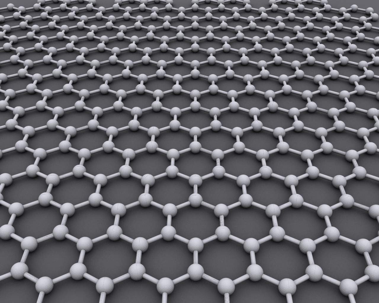
Graphene () is an allotrope of carbon consisting of a Single-layer materials, single layer of atoms arranged in a hexagonal lattice nanostructure. "Carbon nanostructures for electromagnetic shielding applications", Mohammed Arif Poothanari, Sabu Thomas, et al., ''Industrial Applications of Nanomaterials'', 2019. "Carbon nanostructures include various low-dimensional allotropes of carbon including carbon black (CB), carbon fiber, carbon nanotubes (CNTs), fullerene, and graphene." The name is derived from "graphite" and the suffix -ene, reflecting the fact that the graphite allotrope of carbon contains numerous double bonds. Each atom in a graphene sheet is connected to its three nearest neighbors by a strong σ-bond, and contributes to a valence band one electron that extends over the whole sheet. This is the same type of b ... [...More Info...] [...Related Items...] OR: [Wikipedia] [Google] [Baidu] |
Raman Spectroscopy
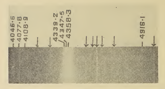
Raman spectroscopy () (named after Indian physicist C. V. Raman) is a spectroscopic technique typically used to determine vibrational modes of molecules, although rotational and other low-frequency modes of systems may also be observed. Raman spectroscopy is commonly used in chemistry to provide a structural fingerprint by which molecules can be identified. Raman spectroscopy relies upon inelastic scattering of photons, known as Raman scattering. A source of monochromatic light, usually from a laser in the visible, near infrared, or near ultraviolet range is used, although X-rays can also be used. The laser light interacts with molecular vibrations, phonons or other excitations in the system, resulting in the energy of the laser photons being shifted up or down. The shift in energy gives information about the vibrational modes in the system. Infrared spectroscopy typically yields similar yet complementary information. Typically, a sample is illuminated with a laser beam ... [...More Info...] [...Related Items...] OR: [Wikipedia] [Google] [Baidu] |
Epitaxy
Epitaxy refers to a type of crystal growth or material deposition in which new crystalline layers are formed with one or more well-defined orientations with respect to the crystalline seed layer. The deposited crystalline film is called an epitaxial film or epitaxial layer. The relative orientation(s) of the epitaxial layer to the seed layer is defined in terms of the orientation of the crystal lattice of each material. For most epitaxial growths, the new layer is usually crystalline and each crystallographic domain of the overlayer must have a well-defined orientation relative to the substrate crystal structure. Epitaxy can involve single-crystal structures, although grain-to-grain epitaxy has been observed in granular films. For most technological applications, single domain epitaxy, which is the growth of an overlayer crystal with one well-defined orientation with respect to the substrate crystal, is preferred. Epitaxy can also play an important role while growing superlatti ... [...More Info...] [...Related Items...] OR: [Wikipedia] [Google] [Baidu] |
Glass
Glass is a non-Crystallinity, crystalline, often transparency and translucency, transparent, amorphous solid that has widespread practical, technological, and decorative use in, for example, window panes, tableware, and optics. Glass is most often formed by rapid cooling (quenching) of the Melting, molten form; some glasses such as volcanic glass are naturally occurring. The most familiar, and historically the oldest, types of manufactured glass are "silicate glasses" based on the chemical compound silicon dioxide, silica (silicon dioxide, or quartz), the primary constituent of sand. Soda–lime glass, containing around 70% silica, accounts for around 90% of manufactured glass. The term ''glass'', in popular usage, is often used to refer only to this type of material, although silica-free glasses often have desirable properties for applications in modern communications technology. Some objects, such as drinking glasses and glasses, eyeglasses, are so commonly made of silicate- ... [...More Info...] [...Related Items...] OR: [Wikipedia] [Google] [Baidu] |
Thermal Conductivity
The thermal conductivity of a material is a measure of its ability to conduct heat. It is commonly denoted by k, \lambda, or \kappa. Heat transfer occurs at a lower rate in materials of low thermal conductivity than in materials of high thermal conductivity. For instance, metals typically have high thermal conductivity and are very efficient at conducting heat, while the opposite is true for insulating materials like Rockwool or Styrofoam. Correspondingly, materials of high thermal conductivity are widely used in heat sink applications, and materials of low thermal conductivity are used as thermal insulation. The reciprocal of thermal conductivity is called thermal resistivity. The defining equation for thermal conductivity is \mathbf = - k \nabla T, where \mathbf is the heat flux, k is the thermal conductivity, and \nabla T is the temperature gradient. This is known as Fourier's Law for heat conduction. Although commonly expressed as a scalar, the most general form of ... [...More Info...] [...Related Items...] OR: [Wikipedia] [Google] [Baidu] |
Electrical Conductivity
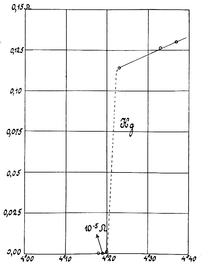
Electrical resistivity (also called specific electrical resistance or volume resistivity) is a fundamental property of a material that measures how strongly it resists electric current. A low resistivity indicates a material that readily allows electric current. Resistivity is commonly represented by the Greek letter (rho). The SI unit of electrical resistivity is the ohm- meter (Ω⋅m). For example, if a solid cube of material has sheet contacts on two opposite faces, and the resistance between these contacts is , then the resistivity of the material is . Electrical conductivity or specific conductance is the reciprocal of electrical resistivity. It represents a material's ability to conduct electric current. It is commonly signified by the Greek letter (sigma), but (kappa) (especially in electrical engineering) and ( gamma) are sometimes used. The SI unit of electrical conductivity is siemens per metre (S/m). Resistivity and conductivity are int ... [...More Info...] [...Related Items...] OR: [Wikipedia] [Google] [Baidu] |


